Folding Electronics: Origami Circuit Boards Could Make Tech More Accessible
What if building your own electronics felt more like folding paper? Origami circuit boards are blurring the lines between craft and code, potentially bringing complex tech prototyping into more hands.
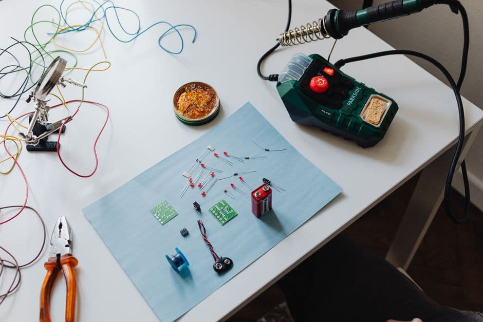
I’ve spent enough time wrestling with soldering irons and staring at microscopic traces to know that making electronics can feel like an impenetrable fortress for many. You need specialized tools, a clean workspace, and a tolerance for smoke. It’s a barrier, plain and simple. But what if a lot of that complexity could be sidestepped, not by making things simpler in terms of function, but simpler in terms of assembly? That’s the tantalizing promise behind the concept of origami circuit boards, which IEEE Spectrum recently explored.
Think about origami. It’s an ancient art form, deeply rooted in craftsmanship, precision, and the ability to transform a flat sheet into something three-dimensional and functional. Now, imagine applying that same folding logic to the intricate pathways of a circuit board. It sounds a bit like science fiction, but researchers are genuinely exploring how to fold conductive materials and components into complex, multi-layered electronic devices. The core idea is to move away from the subtractive manufacturing (milling away material) or additive manufacturing (layer by layer deposition) we typically associate with PCBs, and instead leverage the inherent geometry of folding.
The implications for accessibility are pretty significant. For anyone who’s ever tinkered with Arduino or Raspberry Pi and wished for a more intuitive way to build, this could be a game-changer. Traditional circuit boards are flat. To create more complex, 3D structures, you usually have to stack boards or use specialized connectors, which adds bulk and expense. Origami techniques, however, could allow for integrated 3D configurations right from a folded sheet. Imagine a device that folds up into a compact form factor, or a sensor array that can be deployed by simply unfolding it.
This isn’t about replacing the dense, high-performance boards you find in your smartphone or gaming PC. Those require extreme precision and miniaturization that folding alone can’t easily achieve. Instead, the focus is on applications where flexibility and ease of assembly are paramount, and where a certain degree of bulk is acceptable, or even desirable. Think educational kits, rapid prototyping of novel sensors, or even flexible electronics for wearable applications that can be easily assembled and perhaps even repaired.
One of the challenges in electronics is the sheer variety of components and how they connect. With origami circuit boards, the goal is to design the folding pattern so that when you fold the material, the conductive traces automatically align and connect the embedded components. This could dramatically reduce the need for external wiring and complex soldering. It’s about embedding the connectivity within the structure itself, guided by the folds.
The IEEE Spectrum piece highlights that this is still an area of active research. The materials science involved is crucial. You need substrates that can be folded repeatedly without degrading their conductivity, and conductive inks or materials that can withstand the folding process. Researchers are experimenting with various conductive polymers and nanoparticle inks, as well as novel substrate materials. The ability to precisely control where conductivity exists on the folded material is key.
What excites me is the potential to demystify electronics prototyping. Often, the first hurdle for aspiring makers isn't understanding the code, but the physical construction. If you can learn to fold a circuit board like you learn to fold a paper crane, the barrier to entry lowers considerably. It brings a tactile, almost artistic element back into the process, making it more engaging and less intimidating. It’s about taking complex engineering and presenting it through a familiar, accessible medium.
Consider the educational aspect. Instead of students assembling pre-made kits with breadboards and jumper wires, imagine them designing and folding their own functional circuits. This could teach principles of geometry, material science, and electrical engineering in a hands-on, intuitive way. The resulting devices could be anything from simple light-up cards to more complex robotic components.
Of course, there are hurdles to overcome. Achieving reliable, repeatable connections with folding is non-trivial. The longevity and durability of folded circuits under repeated stress are also key research areas. Furthermore, scaling this from a lab experiment to mass production requires further innovation in manufacturing techniques that can handle precise folding and component integration.
But the vision is compelling. It’s a future where crafting your own technology doesn’t require a cleanroom, but perhaps just a good set of instructions and a steady hand. It bridges the gap between the meticulous craft of traditional arts and the rapid innovation of modern technology. It’s a reminder that sometimes, the most advanced solutions come from looking at familiar concepts in entirely new ways, like the humble fold. This isn’t just about new electronics; it’s about a new way of making electronics, and that’s something worth paying attention to.